The researchers simulated an all perovskite solar cell offering the advantage of effectively harnessing sunlight across a wide range of wavelengths. The device has the potential to achieve an open-circuit voltage of 3.76 V, a short-circuit density of 10.70 mA/cm², and a fill factor of 69.00%.
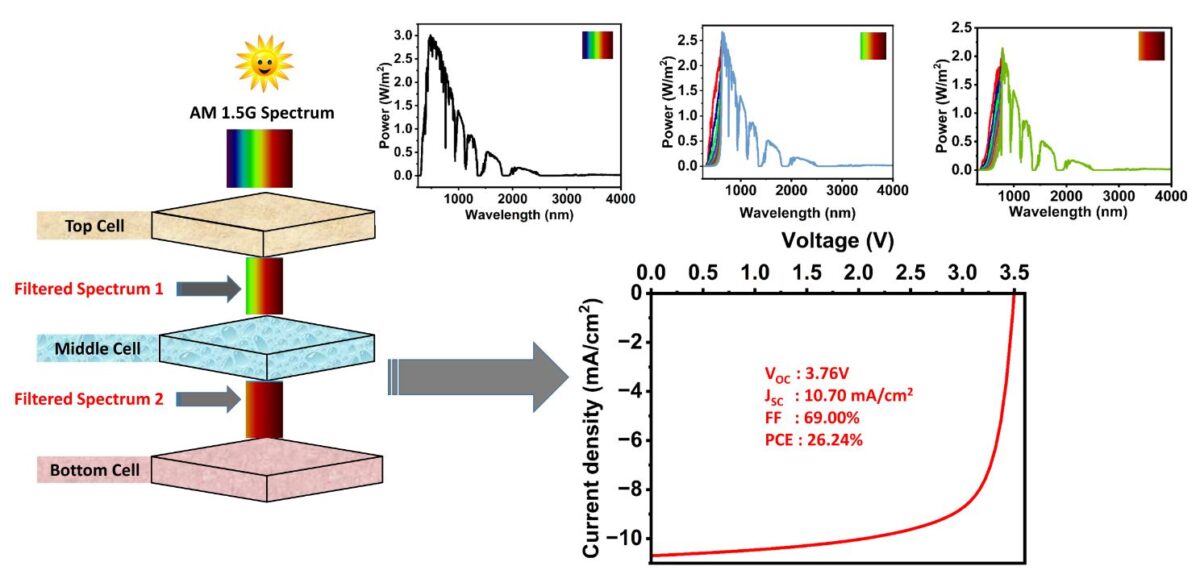
A group of researchers led by the Technology Chitkara University in India has designed a three-junction all-perovskite tandem solar cell (3J-APTSC) that can reportedly achieve a power conversion efficiency of 26.24%.
All perovskite PV devices offer the advantage of effectively harnessing sunlight across a wide range of wavelengths. “By strategically applying two-step filtered spectrum and current matching techniques, our team has fully realized the capabilities of the three-junction tandem solar cell design,” the research's corresponding author, Jaya Madan, told pv magazine.
The scientists used the SCAPS-1D solar cell capacitance software, developed by the University of Ghent, to simulate the novel cell configuration. “This device simulator is known for its reliability in modeling standalone and two-junction tandem solar cells. However, until now, there hasn't been a method for simulating three-junction tandem solar cells using SCAPS-1D. Thus, our work fills this gap.”
The solar cell relies on a 287 nm-thick top cell comprising an electron transport layer (ETL) based on tin oxide (SnO2) and buckminsterfullerene (C60), a perovskite active layer with a bandgap of 1.99 eV, and a hole transport layer (HTL) made of methyl-substituted carbazole (Me-4PACz).
Moving down the tandem structure, the 500 nm-thick middle cell features a perovskite absorber layer with a bandgap of 1.6 eV. The top and bottom subcells are interconnected through an indium tin oxide (ITO) layer, facilitating efficient charge transport between the layers. The 670 nm-thick subcell integrates a perovskite absorber with a bandgap of 1.20 eV.
The performance of the cell was simulated under standard illumination conditions and, according to the scientists, it achieved remarkable photovoltaic parameters. The device reached an efficiency of 26.24%, an open-circuit voltage of 3.76 V, a short-circuit density of 10.70 mA/cm², and a fill factor of 69.00%.
The researchers explained that the precise determination of the filtered spectrum and the current matching points played a crucial role in the cell optimization.
From: PV Magazine
 Chinese
 English